
As the integrated circuit industry keeps evolving, the complexity of chip connections has grown significantly. Traditional printed circuit board (PCB) technology is now facing limitations when it comes to meeting the needs of higher-frequency and faster-speed applications. Ensuring stable and reliable connections between high-speed and high-density chips has become crucial.
Furthermore, as the power consumption of chips continues to increase, so does the amount of heat generated. This necessitates an efficient cooling system to keep the chips functioning properly.
As a result, a new type of PCB called the interposer PCB has come into existence.
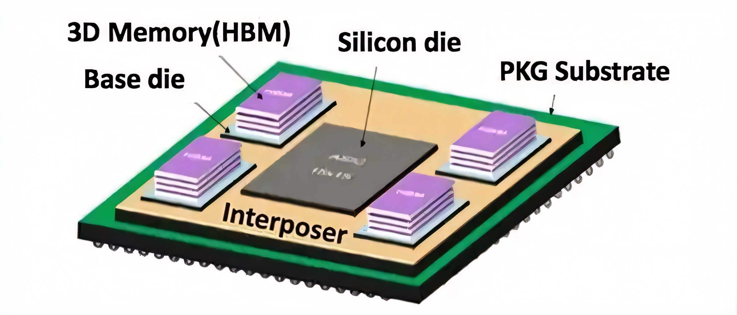
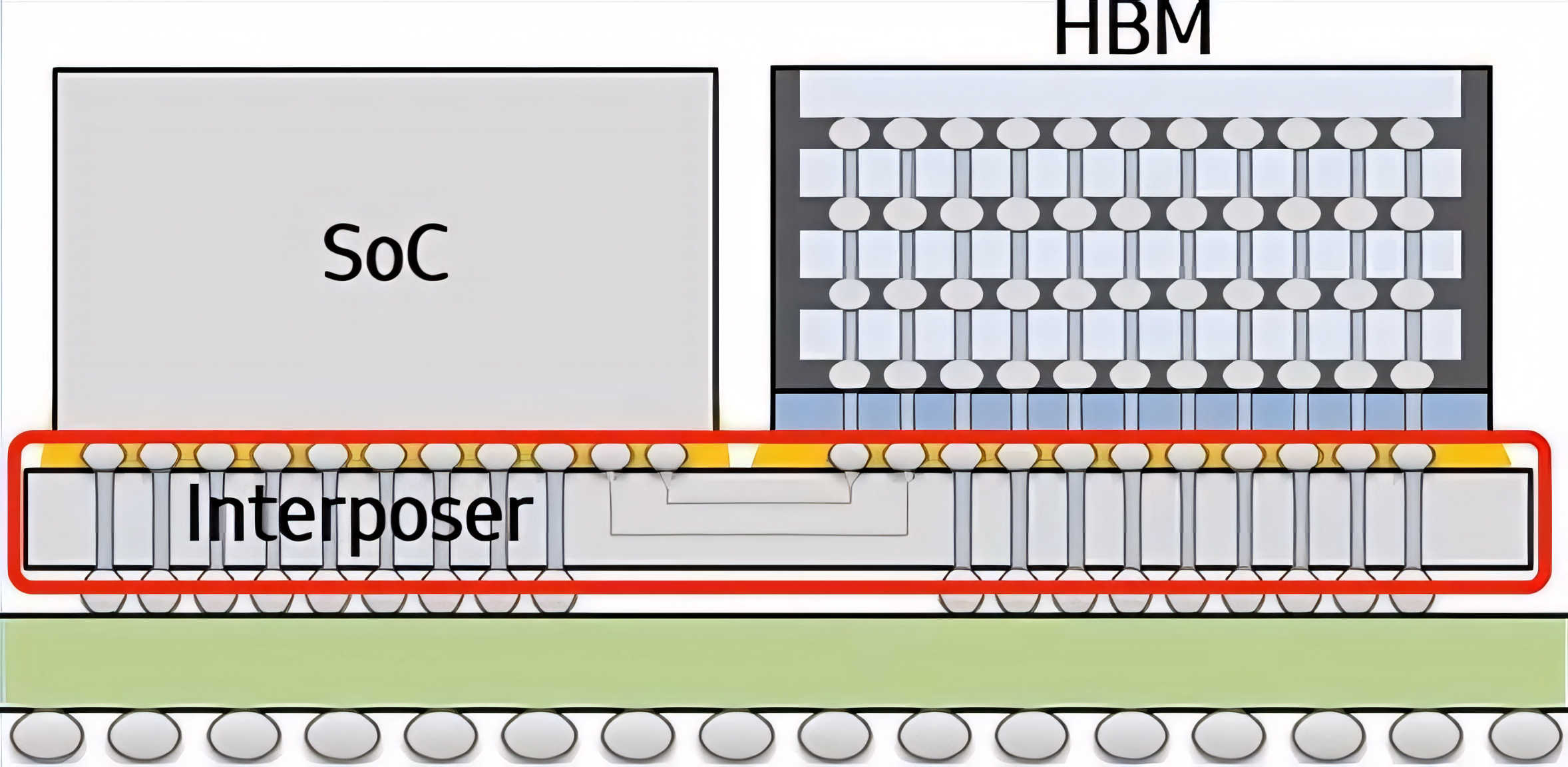
An interposer PCB is essentially a highly precise, multi-layered PCB that allows for arbitrary interconnection. It plays a key role in connecting and integrating various electronic components, acting as a bridge between different chips. Electrical connections are established through pad leads, micro bumps (uBump), and routing within the intermediary layer. The intermediary layer uses through-silicon vias (TSV) to connect the upper and lower layers.
This PCB's design features inner layers interconnected with the outer layers via laser microvias and dense routing, creating a multi-structured board with BGA connections on the top side and pad connections on the bottom side.
Interposer PCBs are invaluable in enhancing various performance aspects of integrated circuits.
Firstly, interposer PCBs offer higher connection speeds and reliability for semiconductor products. Made from high-performance materials, these PCBs enable short-distance, high-density connections between integrated circuits, significantly boosting chip data transmission rates.
Secondly, interposer PCB technology tackles signal integrity and power consumption issues. By employing interposer technology, signal pins can be directly connected to the interposer layer, reducing the length of signal transmission paths, thereby minimizing signal loss and improving signal integrity.
Thirdly, the interposer layer also serves a thermal management function, effectively lowering chip temperatures.
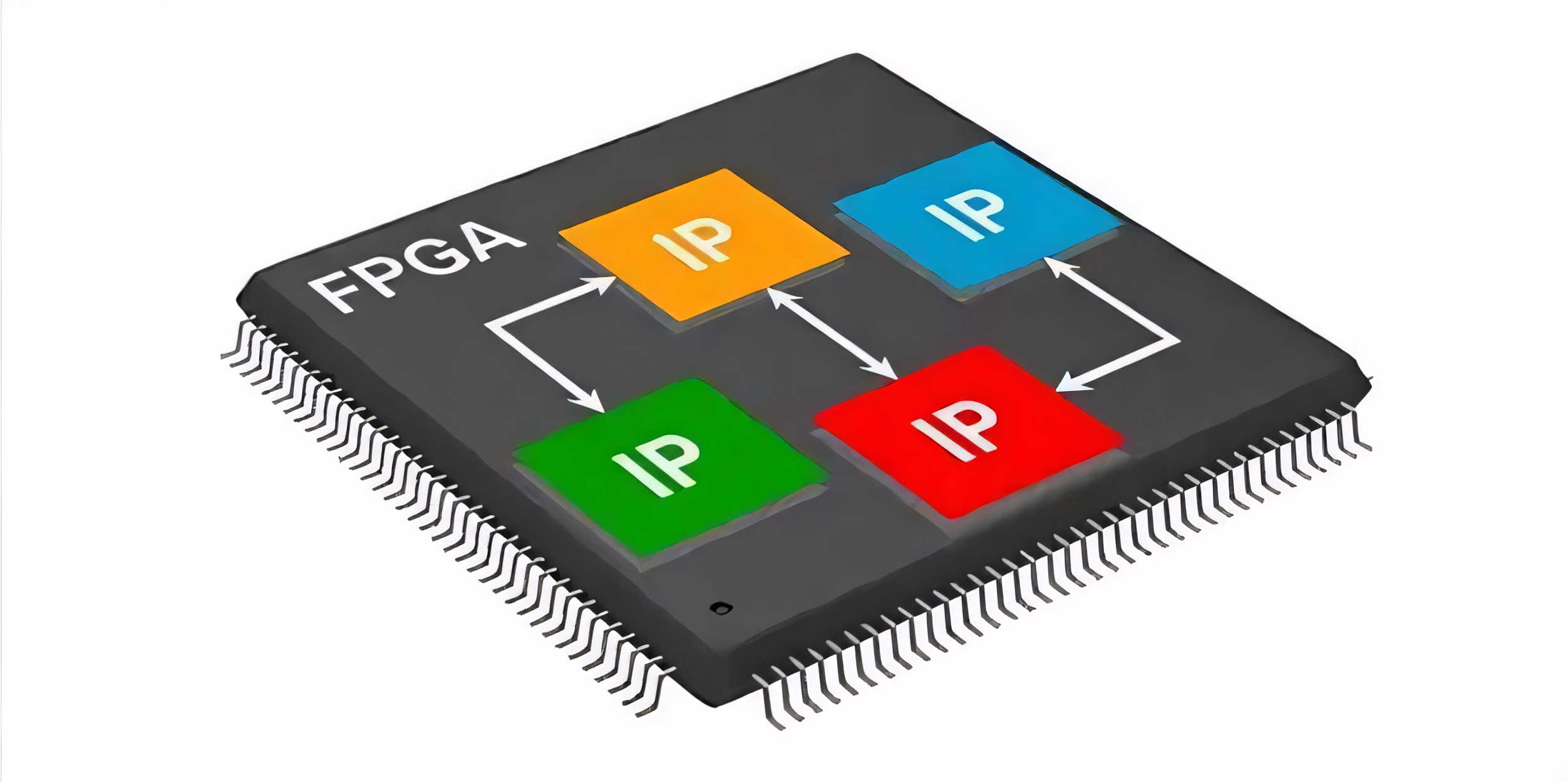
Lastly, interposer PCB technology facilitates the connection between heterogeneous integrated circuits. By placing integrated circuits with different functionalities on the same interposer layer, it enables interconnections between various chips, thus enhancing the overall performance and efficiency of semiconductor products.
In summary, interposer PCBs are extensively used in areas like high-performance computing, artificial intelligence, data centers, and communications. In high-performance computing systems, interposer technology can connect multiple processing chips, enabling larger-scale computing capabilities. In the field of artificial intelligence, interposer technology facilitates interconnections between different chips, enhancing the training and inference speeds of neural networks. For data center and communication applications, interposer technology offers higher transmission rates and bandwidth to meet the demands of big data processing and high-speed communication.
As a leading manufacturer of high-end HDI PCBs, PCBWay stays ahead of market trends. In response to the pressing need from clients for high-order arbitrary interconnection (Anylayer) HDI boards, our product research institute has worked hard to overcome technical hurdles, finally achieving the successful development of high-layer, high-order arbitrary interconnection interposer PCBs.
Here, we’ll showcase the details of this high-precision circuit product using the 24-layer, 6-order Anylayer HDI PCB as an example.
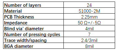
1. Product Parameters
2. Product Structure
3. Technical Challenges
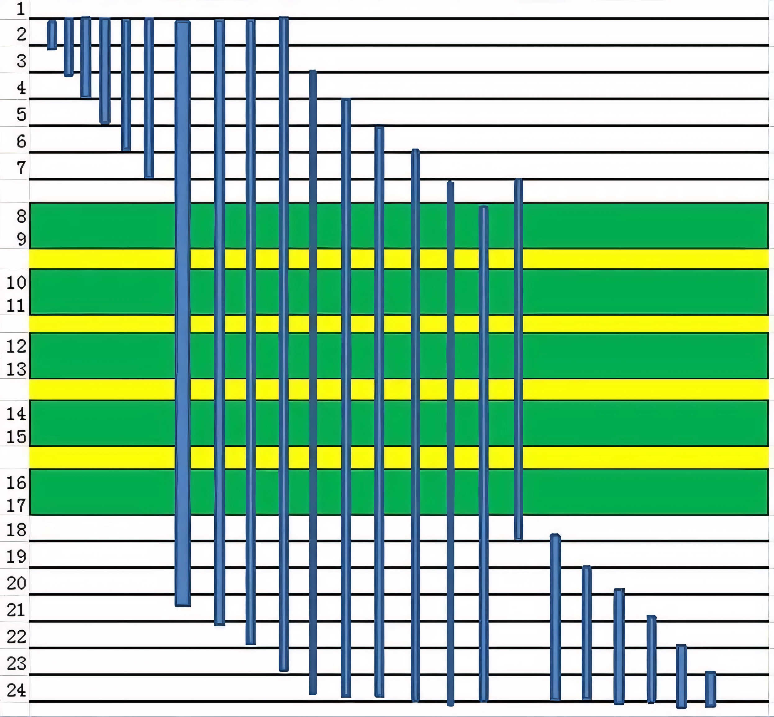
Challenge 1: The buried via PCB thickness from L7 to L18 is 1.0 mm, with a mechanical through-hole diameter of 0.1 mm, resulting in a hole aspect ratio of 10:1, making mechanical drilling challenging.
Challenge 2: The BGA pitch is 0.35 mm, and the distance from the hole to the conductor trace is 0.13 mm, which can lead to misalignment during multiple laminations.
Challenge 3: The trace width/spacing is 2.4/3 mil, and it features dense routing. Below are some routing diagrams.
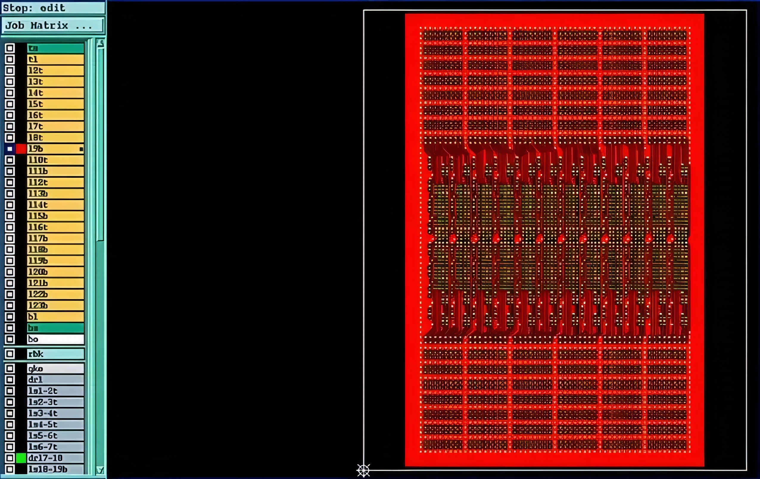
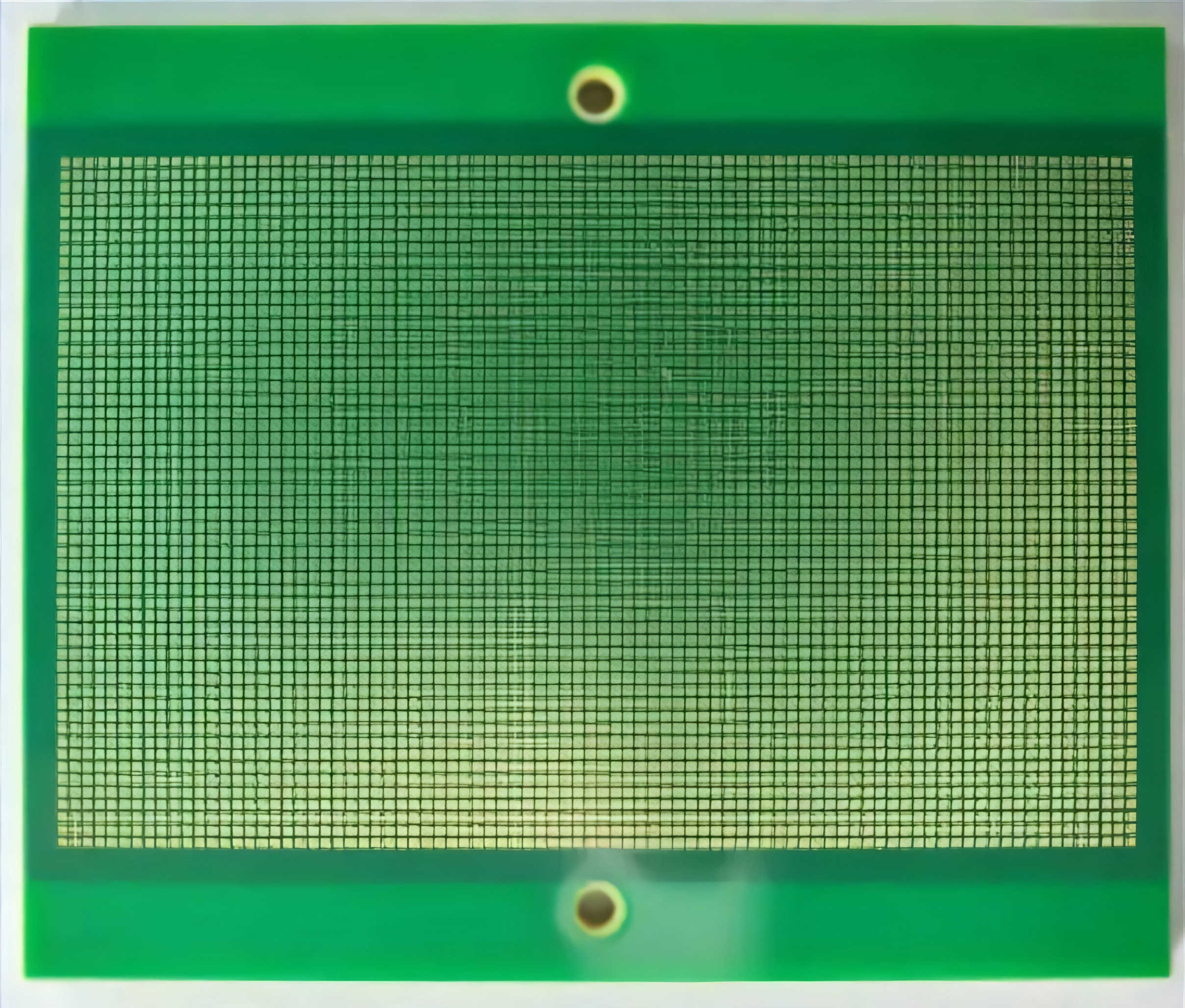
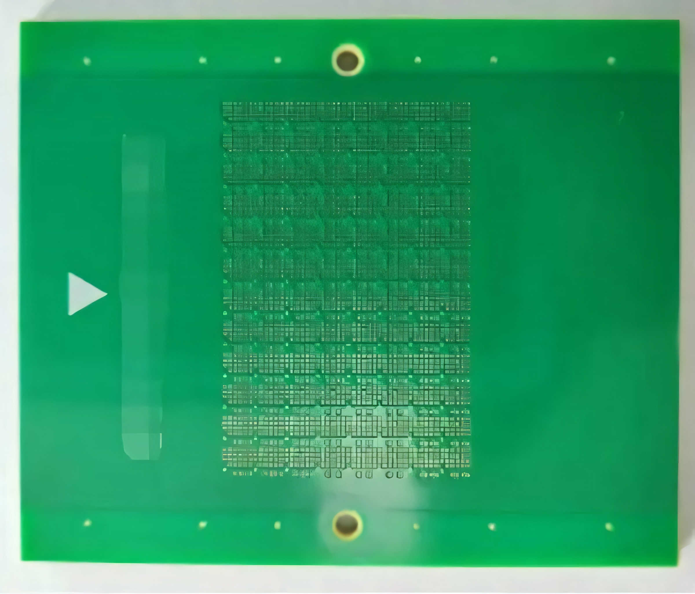
4. Finished Product Pictures
Modular Parts Box,Plastic Parts Containers,Plastic Parts Storage Bins,Plastic Bins For Parts
Jiangsu Ru Shun plastic industry Co., LTD , https://www.rushunsuye.com